Thiel Research Group
Surfaces
Semiconductors and InsulatorsSilicon
Metallic Alloys
NiAl(110)
Quasicyrstal
Metallic Glass
Pure Metals
Silver
Reseach Interests
Thin Films on Silicon Surfaces
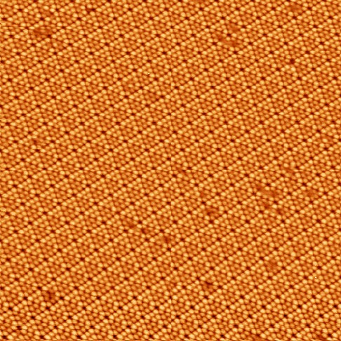
Clean Si(111) reconstructed to (7x7); STM image 50 x 50 nm2
Ag on Si(111)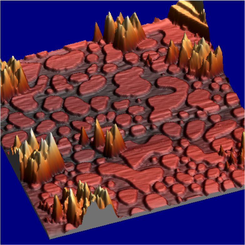
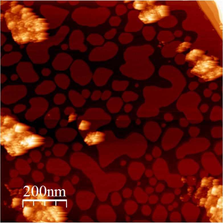
This is Ag on top of Ag/Si(111) - (√3x√3)R30° at 250K forming large, rough, islands. The interesting part about this image is the sheer size and roughness of the islands. The silver aggregates to form a highly faceted <111>-type structures with steps and terracesIn the actual island. The left image is a 3-dimensional version of the right image; 1x1 mm2, -2 V, 0.2 nA. Please see publication for more information.
TopThin Films on NiAl(110)
Au and Ag island morphologies vs. deposition temperature.
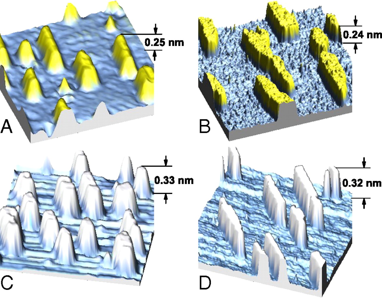 Au/NiAl(110) at 24% areal coverage and flux 8x10⁻⁴ ML/s: (A) 200 K (23x23 nm2; (B) 300 K (100x100 nm2). Ag/NiAl(110) at 20% areal coverage and flux 6x10⁻³ ML/s: (C) 140 K (30x30 nm2); (D) 200 K (100x100 nm2). Please see publication for more information.
LEED images of the clean surface at 120 K
64 eV 111 eV
165 eV 222 eV
Quasicrystal Surfaces
The following article is a great introduction to quasicrystals:
P. A. Thiel, "Quasicrystal Surfaces" Annual Review of Physical Chemisty, 59, 129-152 (2008).
Icosahedral phases can be regarded as quasiperiodic in three dimensions
consisting of clusters of concentric shells containing a few tens of atoms.
The dark star in STM image below is universally interpreted as a hollow
site corresponding to a sliced cluster. The favored terminations in i-Al-Pd-Mn
and i-Al-Cu-Fe consist of pairs of planes, in which the outermost plane
is 90-100 at% Al, and the second plane is roughly half Al and half Pd. The
wo planes are separated by only 0.04 nm, so they are aptly described as
a single rumpled layer with a composite. Please see our publication page for a full list of relevant articles.
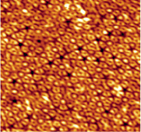
Terrace, 15 x 15 nm2
X-ray photoelectron spectra showing the Zn 2p3/2, Pd 3d, and Al 2p peaks after different environmental treatments.
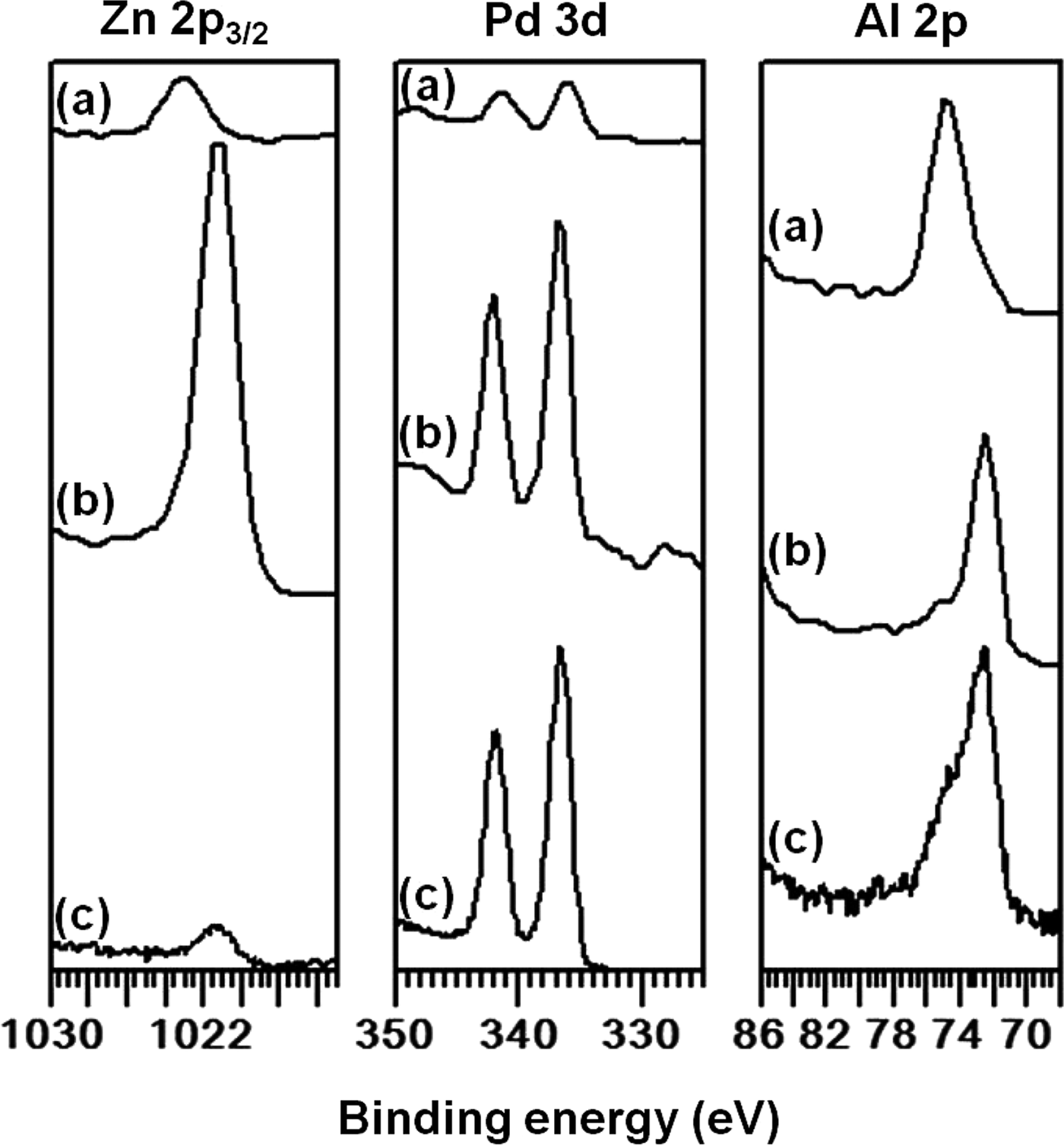
(a) Exposure to air. (b) Cleaning by sputtering in UHV. (c) Oxygen exposure in UHV (300 Langmuirs at room temperature). For each core level, the peaks are normalized to the intensity of the clean surface in (b). Please see publication for more information.
Thin Films on Metallic Glass
Ag on Zr-Ni-Cu-Al as a function of temperature
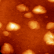
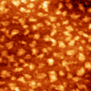
300 K 260 K
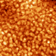
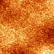
240 K 190 K
STM images following deposition of 12 ML Ag at different substrate temperatures on Bulk Metallic Glass surface. Image size: 250 nm x 250 nm. Please see publication for more information.
Chalcogens on Low-Index Coinage Metal Surfaces
Coarsening
S enhanced Ag island coarsening on Ag(100)
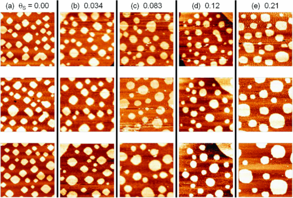
STM images showing Ag island coarsening at different S coverages at 300 K. Ag coverages are all 0.3 ML, and STM images are 50 x 50 nm2. S coverage increases moving to the right (value given in header), and time after deposition increases moving down a column (with the last row of images recorded about 3 hrs after Ag and 2 hrs after S.
Please see publication for more information.
See also earlier Oxygen on Silver STM images.
Structures
Sulfur induced reconstruction of Ag(100)(√17x√17)R14°
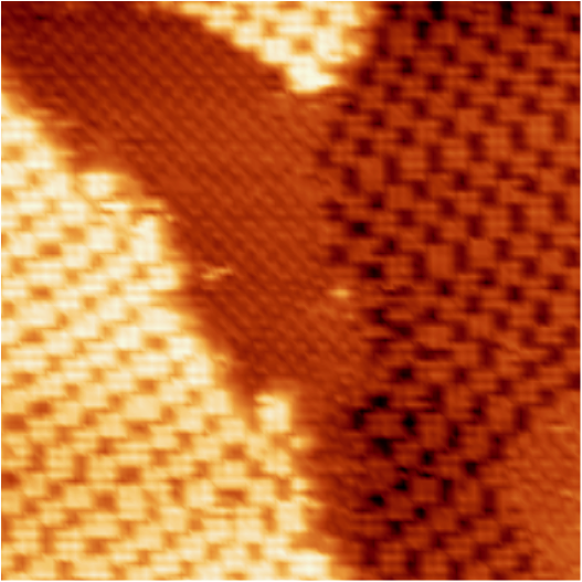
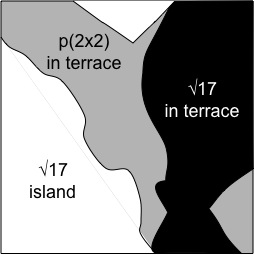
After sulfur adsorption at 120 K and heating to 300 K, a mixture of the √17 reconstruction and p(2x2) structure. STM image 25x25 nm2. Please see publication for more information.
"Dot-Row" structure of S/Ag(111)
A strong case, based partly on energy calculations and the height of the dots in STM, can be made for assigning the dots as Ag3S3 clusters.
0.4 ML S/Ag(111), 200 K, 8x8 nm2
0.1 ML S/Ag(111), 60x60 nm2
Several hours after adsorption at 200 K ends and after heating to 300 K and re-cooling to 200 K. Please see publication for more information.